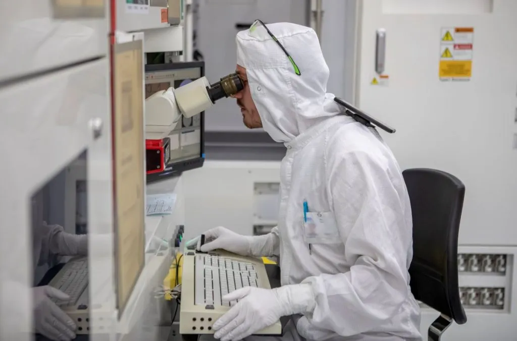
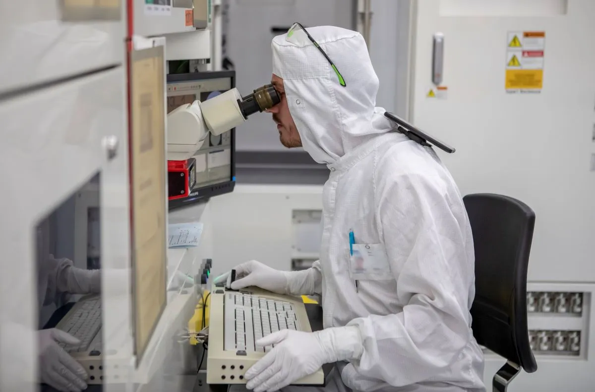
In-fab semiconductor metrology and inspection technologies support semiconductor manufacturing steps during processing in the fab.
They are used for either process verification or process control. During the latter a product sample is processed, relevant properties are measured and the process is adjusted to bring the next processed sample closer to its specification.
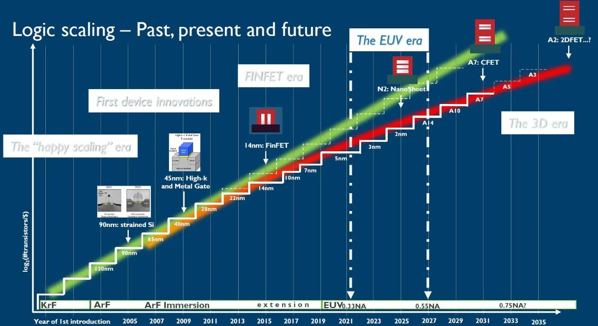
Figure 1: A view on imec’s logic scaling roadmap since 1986, linked to notable innovations in lithography and device technologies
Accuracy is the main requirement for metrology tool development, which focuses on measuring and quantifying dimensions – such as critical dimensions of patterned structures. Different criteria apply to inspection, aimed at detecting a wide variety of defect types on a wafer at multiple process stages. Here, detectability of defects at the wafer scale is essential, without the need for measuring dimensions. For both metrology and inspection, operation in the fab additionally translates into specs for precision and throughput, while meeting cost and sustainability criteria.
Optical metrology domination
The timespan between 1986 and 2005 is part of the so-called ‘happy scaling era’: the semiconductor industry advanced merely by the dimensional scaling of chip components, supported by KrF-based lithography systems that operate using light at a wavelength of 248nm during exposure in the scanner.
The metrology and inspection landscape was dominated by optical tools such as optical microscopes and ellipsometers, using light sources to interact with the structures being measured. Initially, most of the work was done manually and with a small number of product samples, limiting the use of metrology and inspection to process verification.
When dimensions became smaller and the logic roadmap approached the 130nm technology node, e-beam-based techniques were introduced to answer more stringent resolution requirements: CD scanning electron microscopy (CD-SEM) for measuring line widths, review SEM for defect ‘review’ and classification, and inspection SEM for wafer-level defect inspection.
Dimensional scaling also reduced the budget available for overlay between successively patterned layers. Fortunately, evolutions in metrology techniques throughout the 1990s gradually brought more automation and sampling, and higher accuracy. This allowed the semiconductor industry to start using overlay measurements for controlling and correcting any misplacements between successive layers.
Toward the end of the happy scaling era scatterometry was introduced, a diffraction-based optical metrology tool relying on the scattering of light by repetitive structures. This technique provided not only line width information at smaller pitches, but also additional information such as the height and profile of patterned structures. Being non-destructive and high throughput, it rapidly became a fab-critical tool for monitoring advanced processes.
Device innovations
From the early 2000s to around 2011 we observed a slight deviation from the ‘perfect’ scaling path according to Moore’s Law. To keep up with Moore’s Law and maintain performance improvement, strain was induced into Si conduction channels of 90nm mosfet devices. This mobility booster was enabled by, for example, adding SiGe stressors in source/drain regions. Also, from the 45nm node onwards, the traditional SiO2/poly-Si based gate stack was replaced by a high-k/metal gate stack to allow the gate to regain control over the channel, as such addressing short channel effects.
Introducing novel materials as an additional knob to boost performance presented a new challenge for metrology: the need to characterise these materials. That’s when X-ray-based techniques entered the fab: in-line X-ray diffraction for characterising strained channels, and in-line X-ray photoelectron spectroscopy for high-k/metal gates.
An increase in resolution required by the continued dimensional scaling was provided by ArF-based lithography systems, using light at smaller wavelength (193nm) compared to KrF-based systems during exposure in the scanner. These 193nm ‘dry’ lithography systems were followed by 193nm immersion lithography scanners to enable even smaller pitches. But the presence of water created so-called bubble defects that posed additional challenges for inspection tools: the need to detect small and process induced defects over the full wafer.
The 193nm immersion lithography triggered the first use of broadband plasma tools within the fab. These tools are still in use for characterising the most advanced device structures and for back-end-of-line inspection.
The finfet era
The finfet era marks the first significant architectural shift in transistor device history. In a finfet, the conduction channel between source and drain terminals is in the form of a three-dimensional fin, and the gate wraps around this channel. This multi-gate structure was introduced in the 22nm node to further reduce short-channel effects, which continued to degrade transistor performance at reduced gate length.

The advent of 3D device technology heralded the beginning of the 3D metrology era. Scatterometry, which was introduced in the first period, turned out to be fully effective in the 3D space. Also, the metrology community started considering hybrid metrology: combining different techniques – such as optical critical dimension metrology and CD-SEM – to extract more information or in a more accurate way.
In the same period double-patterning techniques were used to extend 193nm lithography in anticipation of extreme ultraviolet (EUV) lithography being ready for mass production. With double (or multi-) patterning, a chip pattern is split into two (or more) ‘simpler’ masks. This allows printing smaller features, but increases the complexity and cost of the chip manufacturing process.
More specifically, double patterning significantly increases the requirements for overlay between the two successively patterned layers, reducing the budget for overlay errors. That’s when imec and the metrology community introduced the edge placement error (EPE) metric, describing how the placement of the various structures deviates from the intended design. Metrologists had to find a way to measure all the parameters that enter the EPE equation. They also brought in new algorithms for CD-SEM – as to characterise the two different CD populations that were created by the two separate lithography and patterning steps.
The EUV era
In 2019 the semiconductor industry used Low NA (0.33NA) EUV lithography and patterning for the first time in the mass production of logic chips of the 7nm node. Using EUV light of 13.5nm during exposure in the lithography scanner significantly reduces the number of photons hitting the wafer, compared to 193nm lithography. This induces random effects on the printed structures, referred to as the stochastic effects of EUV lithography. These stochastic effects can be grouped into two categories, each of which necessitated innovations in metrology in understanding these effects.
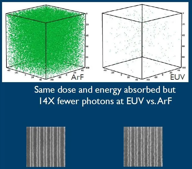
Figure 2: (Top) the reduced number of photons during EUV exposure causes stochastics effects such as (bottom) increased line roughness
First, stochastic effects have a severe impact on the line roughness, translating into increased line edge roughness and top line roughness. Measuring line edge roughness has been addressed by improved CD-SEM techniques, optimised to measure so-called unbiased roughness. By eliminating noise coming from the SEM these measurements could provide a better estimate of the true feature roughness. Characterising top line roughness, on the other hand, was facilitated by AFM.
A second aspect is the presence of stochastic defects, failures that manifest as random line bridges or breaks, or as closing or bridging contact holes. This called for techniques that can both detect extremely small defects (of the order of 10nm and less) and map a large area of the wafer . Optical inspection techniques allow to map a large area but are challenged by the small scale of the defect. E-beam, on the other hand, is a very powerful technique for detecting small defects, but it lacks the throughput for mapping a full wafer. The answer is to combine both techniques to characterise EUV printed defects and define what is called the failure-free process window for EUV lithography.
The future metrology
Dimensional scaling remains an essential pillar in continuing the logic roadmap and unlocking the next wave of AI. Industry continues to use 0.33NA EUV lithography to print the critical layers of the most advanced nodes, that is, 3nm and 2nm logic nodes. Meanwhile, imec and its ecosystem partners have made great strides in readying High NA (0.55NA) EUV lithography and patterning technologies to enable sub-2nm nodes, ensuring increased resolution, process simplification (by reducing the need for multi-patterning), and design flexibility (through the introduction of 1.5D, 2D and curvilinear geometries).
Innovations in patterning are complemented by even more disruptive innovations in device architectures and materials. Gate-all-around nanosheet transistors have been introduced in commercial compute systems and will most likely be succeeded by complementary fets (cfets) from the A7 node onwards. Device architectures will as such increasingly move towards the third dimension. This trend is also defining the future memory landscape – with 3D NAND as the workhorse storage system and DRAM evolving towards 3D architectures. The third dimension additionally enables new chip interconnect architectures. Overall, future compute systems will increasingly rely on 3D integration technologies, including die-to-wafer and wafer-to-wafer hybrid bonding technologies.
Requirements for scaling
All these future options translate into grand challenges and opportunities for metrology and inspection. In terms of ‘xy scaling’ – enabled by advanced lithography and patterning – challenges include the need for increased xy resolution, the characterisation of curvilinear shapes, the ability to detect tiny defects on large wafer areas and the need for vertical sensitivity to characterise structures with varying profiles. ‘Z scaling’ – enabled by 3D devices and 3D integration technologies –is about characterising multilayers and high aspect ratio structures, ‘seeing through’ opaque materials, dealing with topographies at different scales, and measuring edges and backsides of wafers.
These challenges form the basis of imec’s roadmap for metrology, inspection and characterisation, which details when the technologies needed to address these challenges, and when they should be ready and mature for industry.
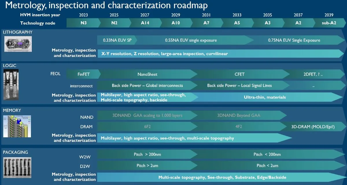
Figure 3: Imec’s metrology, inspection and characterisation roadmap in support of advanced lithography, logic, memory and packaging technologies
Two important evolutions will help shape that roadmap. First, developments are ongoing to extend hardware for improved sensitivity: e-beam metrology with electrons at higher electron volt to improve resolution, optical metrology with photons at smaller wavelengths to detect tiny defects and X-rays to probe deeper into silicon. At the same time innovations are being explored to further boost throughput while keeping ultimate resolution and defect sensitivity: the potential of both multi-head atomic force microscopy and multi e-beam inspection has recently been demonstrated for detecting tiny defects at very high throughput.
Second, gaps are being filled by making greater use of data and algorithms to boost metrology performance. A first example is the use of AI-based algorithms to de-noise incoming measurement data such as e-beam images. Another example is referred to as virtual metrology (or ‘measure-less’ metrology): data measured with a physical metrology tool is complemented and extended with data coming from a virtual metrology model. The latter leverages the conditions of a process tool (for example, power, temperature, flow rate) – as measured by sensors that are attached to the tool – to predict the outcome of a metrology measurement.
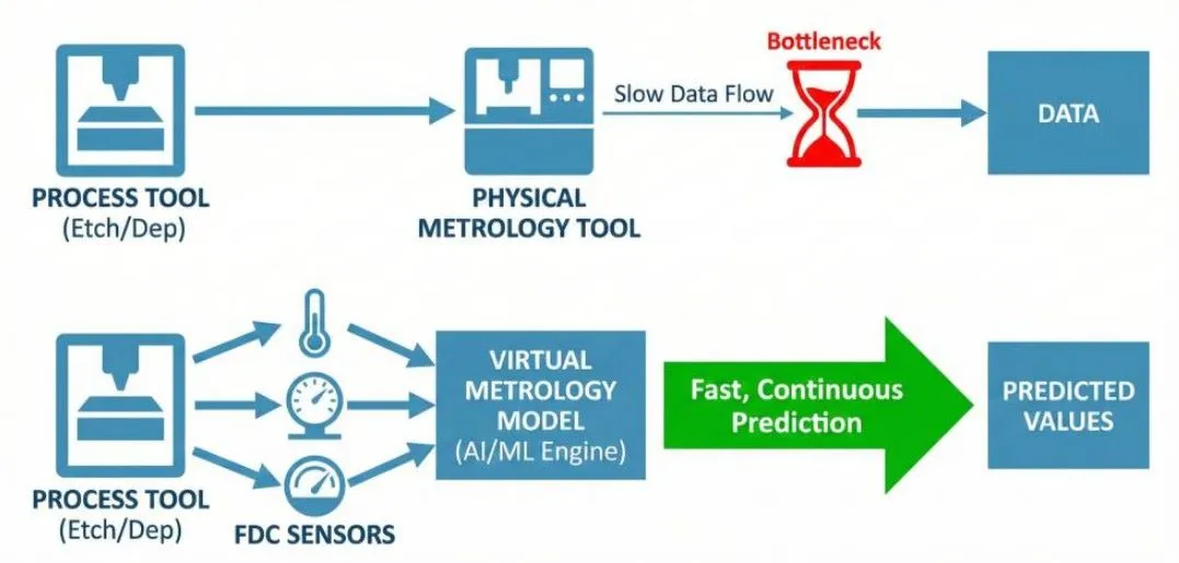

Figure 4: The principle of virtual metrology
Reducing the carbon footprint
Present and future developments also focus on reducing the carbon footprint of metrology and inspection. Imec used its imec.netzero virtual fab model to quantify the share of metrology in the environmental impact of manufacturing the 28nm logic node. Compared to other process areas (such as etch and deposition), the contribution of metrology to overall emissions was found to be relatively small. Nevertheless, measuring accurately at the right process steps is key in improving process yield and reducing waste, highlighting the role metrology should play in reducing the environmental impact of chip manufacturing.
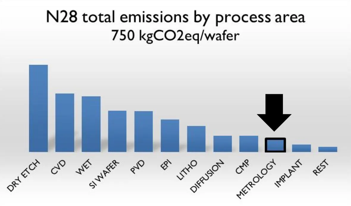
Figure 5: N28 total emissions by process area, generated by the imec.netzero v6.1.57 web app
Wrapping up 40 years of metrology shows how new metrology and inspection techniques have emerged, thereby diversifying the metrology toolbox to address the continued dimensional scaling and increase in process complexity.
The future technology roadmap will further diversify this toolbox, complemented with innovations in existing hardware and an increase in the use of data.
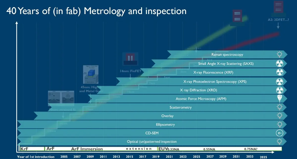
Figure 6: Metrology and inspection techniques adopted over the last 40 years
The future
The next 40 years should continue to bring exciting opportunities to the metrology community. But it also raises questions, for example, about the increased level of automation and role of AI in metrology: how will we guarantee the physical meaning of measured data? What will be the role of metrology experts? Which new sensors will we need to attach to our metrology tools to further boost virtual metrology? Are there more lab techniques to be deployed in the fabs?
Imec will continue expanding its metrology ecosystem to help monitor and characterise advanced technology platforms for logic, memory, lithography and packaging. This metrology ecosystem will also support the EU-funded NanoIC pilot line that is hosted by imec.
About The Author
Anne-Laure Charley is R&D metrology manager at imec and Philippe Leray is vice-president R&D advanced patterning development
See: Metrology and inspection equipment market tops $18bn